
Combinational circuit
Each output depends entirely on the immediate (present) inputs.
Sequential circuit
Each output depends on both present inputs and state
Analysis Procedure
- Label inputs and outputs
- Obtain the functions of intermediate points and the outputs
- Draw the truth table
- Deduce the functionality of circuit
Combinational circuit design methods:
- Gate level design method (with logic gates)
- Block level design method (with functional blocks)
Design methods use logic gates and function blocks available as Integrated Circuit (IC) chips. Types of IC chips based on packing density: SSI, MSI, LSI, VLSI, ULSI.
Main objectives:
- Reduce cost (number of gates for small circuits, number of IC packages for complex circuits)
- Increase speed
- Design simplicity (block reuse)
Gate-level design
- State problem
- Determine label inputs and outputs of circuit
- Draw truth table
- Obtain simplified Boolean functions
- Draw logic diagram
Block-Level Design
More complex circuits are built using block-level methods. We can use 4-bit parallel adders as building blocks, we can create the following:
- BCD-to-Excess-3 Code Converter
- 16-bit Parallel Adder

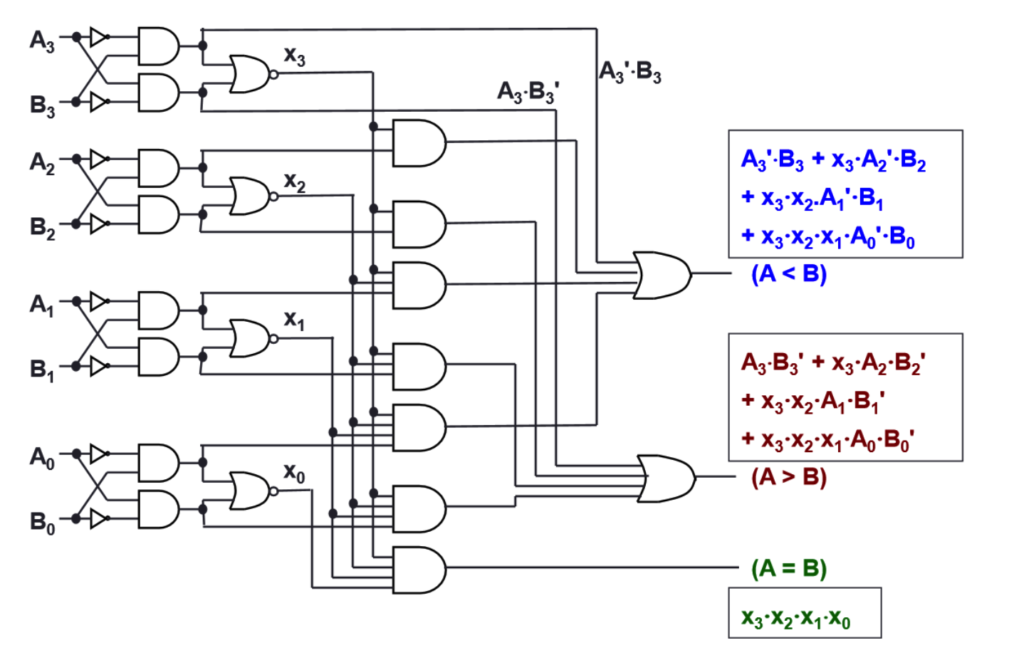
Magnitude Comparator
Compares 2 unsigned values
to check
Circuit delay
Given a logic gate with delay
, if inputs are stable at times , then the earliest time in which the output will be stable is: